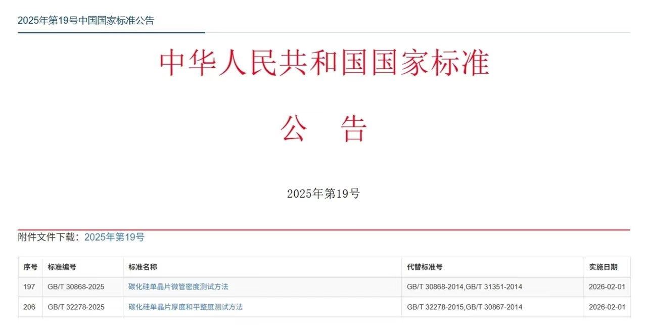
National standards including GB/T 30868-2025 Test method for micropipe density of monocrystalline silicon carbide and GB/T 32278-2025 Test method for thickness and flatness of monocrystalline silicon carbide wafers, developed with the participation of YASC, were approved and released on August 1, 2025 and will be implemented on February 1, 2026, according to the recent China National Standard Announcement 2025 No. 19 made by China’s State Administration for Market Supervision (SAMR) and the Standardization Administration of China (SAC).
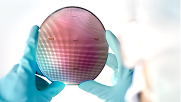
Silicon carbide (SiC), a critical representative third-generation semiconductor material, has had a strategic position in the global energy transition and semiconductor technology upgrades over recent years. Given its excellent physical properties such as wide bandgap, high breakdown field and high thermal conductivity, silicon carbide has demonstrated superior performance advantages over traditional silicon-based materials in high-temperature, high-frequency, high-power scenarios, and become a key material in new energy vehicle (NEV), photovoltaic power generation, smart grid and rail transit fields.
As the demand for standardization is increasing in the silicon carbide industry with rapid iterations in material production processes, device performance and application, there is an urgent need to establish harmonized standards for crystal growth, substrate processing, device process technology and reliability test to ensure product quality and performance consistency.
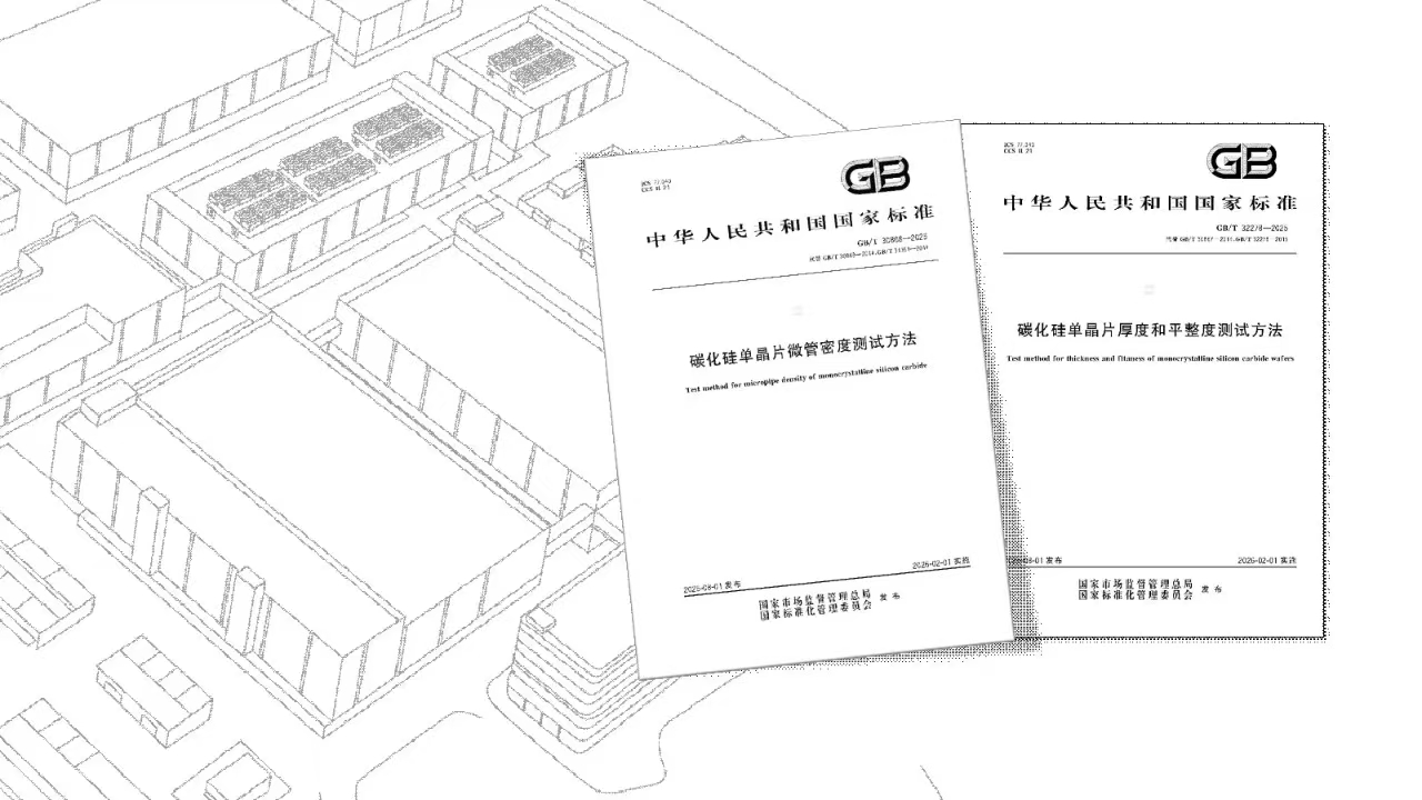
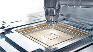
Micropipe density, one of the most important criteria for crystal defects in SiC wafers, directly determines crystallization quality of the epitaxial layer. Thickness and flatness of monocrystalline silicon carbide wafers are also among the most basic parameters of monocrystalline silicon carbide wafers. Accurately measuring the thickness and flatness of monocrystalline silicon carbide wafers matters to improving the quality of SiC substrates, enhancing the quality of epitaxial materials and increasing the yield of device fabrication. The two SiC test method standards, developed with the participation of YASC, have standardized the test methods for monocrystalline silicon carbide wafers, and especially the test methods for thickness and flatness. They will provide unified technical and quality benchmarks for research, production and application, enhance testing efficiency, and thereby improve product manufacturing efficiency and reliability.
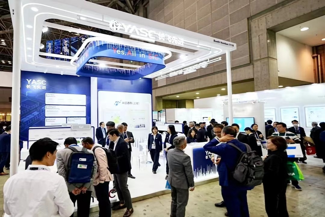
YASC, one of the earliest manufacturers that have researched and developed SiC devices in China, not only attaches great importance to technology R&D and independent innovation, but also plays a leading role in standards development in the SiC industry. Up to now, YASC has participated in setting seven national standards and several industry and association standards released.
YASC will continue to focus on SiC power semiconductor product research, development and manufacturing, take an active part in setting, applying and promoting relevant standards for the silicon carbide industry at home and abroad, and achieve deep integration of guidance on standards and industrial development through the “standard-technology-market” closed loop.