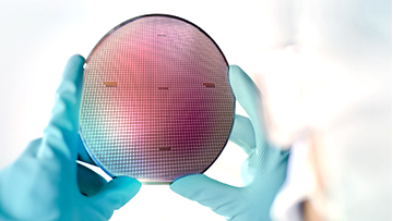
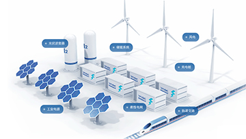
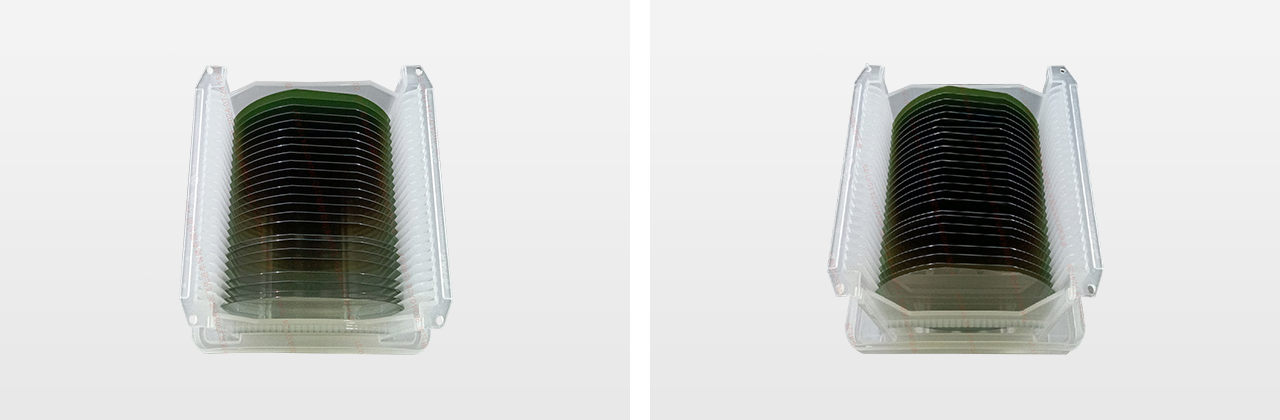
Large size: The large-size SiC epitaxial wafer has a large usable area and lower cost, and can meet the demand for cost reduction and efficiency improvement. Given that 4-inch and 6-inch epitaxial wafers will gradually evolve to 8-inch ones, the large-size epitaxial wafer will account for a growing share each year;
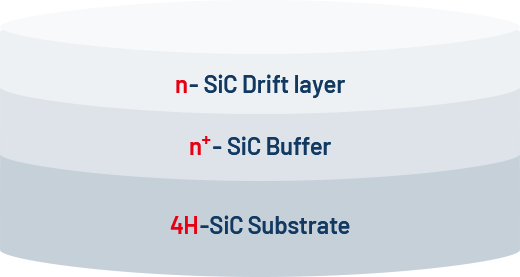
Thick film: The greater the thickness of epitaxial layers, the higher the breakdown voltage of devices. As it can address the needs of high withstand voltage devices, the thick-film epitaxial wafer is also a key research direction in the future.