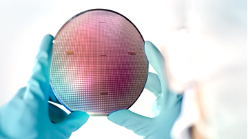
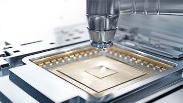
The epitaxial growth technology is an indispensable part of manufacturing silicon carbide (SiC) devices at present. The SiC epitaxial wafer refers to a specific single-crystal film grown through the epitaxy process on the basis of SiC substrate, which has consistent lattice, high purity and low defects. Today, the metalorganic chemical vapor deposition (MOCVD) is the most popular 4H-SiC epitaxial growth method. The upside is that the method can effectively control gas source flows, reaction chamber temperature and pressure in the growth process, change the film-forming environment, and accurately control the epitaxial growth parameters. The method has the excellent characteristics of good repeatability and moderate equipment size.
Photolithography is an important step in the semiconductor manufacturing process. It uses exposure and development to inscribe geometric structures on the photoresist layer, and then transfers the pattern on the photomask to the substrate through an etching process. Photoresists can be divided into positive and negative photoresists according to their properties. The general photolithography process: HMDS preparation, photoresist application, exposure, development, soft bake, and hard bake.
The etch process is a process that selectively removes unnecessary materials from the wafer surface through physical and chemical reactions to meet the requirements in integrated circuit/chip manufacturing. The etching process can be divided into dry etching and wet etching. Wet etching uses liquid etching media, usually a chemically reactive solution or acid-base mixture, which reacts chemically with the material to be etched to achieve etching; dry etching is a process in which a gaseous chemical etchant is used to react with the material to be etched to form volatile byproducts, which are then removed from the substrate surface.
The thin film deposition process is an important material preparation method to form a uniform, thin and dense thin film structure by physical or chemical deposition on the substrate surface. Common thin film deposition methods include physical vapor deposition (PVD), chemical vapor deposition (CVD), solution method, and atomic layer deposition (ALD).
The ion implantation process is one of the main processes in semiconductor fabrication, and is a method of doping semiconductors. It ionizes impurities into ions and focuses into an ion beam, accelerates in an electric field to obtain very high kinetic energy, and then injects into the surface layer of solid material to achieve doping in order to change the physical properties of the material surface layer.
Backthinning is a process in which the wafer is ground and thinned to certain thickness after the circuit on the wafer surface is manufactured, which has an important impact on subsequent assembly.
MOCVD
Lithography machine
PECVD, furnace
MOCVD
Lithography machine
PECVD, furnace
YASC Smart Manufacturing constantly drives smart manufacturing with a complete set of CIM solutions, aiming to build China’s first Full Auto production system in the third-generation semiconductor Auto3 model. The Smart Manufacturing CIM system covers the entire production process from substrate, wafer fabrication and assembly & test to finished product assembly, and realizes multi-factory, multi-workshop production management and quality traceability.
In the wafer fabrication process, YASC Intelligent Manufacturing integrates the automated equipment, smart planning & scheduling system and MES system. Combined with the intelligent Automatic Material Handling System (AMHS), it transforms the YASC manufacturing facility into a smart ecosystem, allows for smooth flow of material within the production facility through precise collaboration among multiple equipment and systems, streamlines the production process, and increases the overall production capacity of the facility.
YASC Smart Manufacturing utilizes advanced automation and data analytics technologies to optimize and manage lean production, personnel management, process and machine control, and equipment capacity in the semiconductor fabrication process to accomplish the company’s goal of increasing productivity, reducing costs, improving product quality and achieving green sustainable development.