The national standard GB/T 43885-2024 “Silicon carbide epitaxial wafers”, which YASC participated in the development of, was approved and released on April 25, and will be implemented on November 1, 2024, according to the China National Standard Announcement 2024 No. 6 recently made by the State Administration for Market Supervision (SAMR) and the Standardization Administration of China (SAC). This is also the fifth national standard released with the YASC participation in the development.
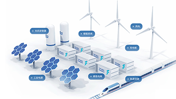
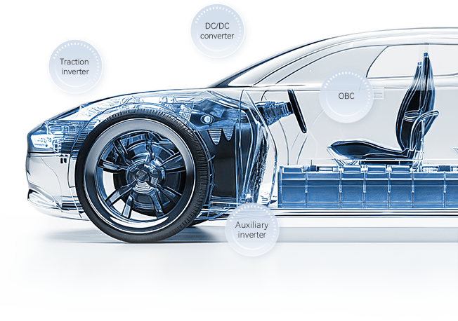
In view of its excellent physical properties like wide bandgap, high breakdown field, high saturation electron drift rate and high thermal conductivity, the silicon carbide (SiC) material as a prime example for third-generation semiconductors has shown broad application prospects in new energy vehicles (NEVs), wind-solar-storage new energy, rail transit and smart grid.
On the emerging track of third-generation semiconductors, countries around the world have unanimously identified silicon carbide as a preferred target for the third-generation semiconductor development and elevated it to a national strategy. After years of development, the SiC conductor is considered as the advanced semiconductor sector most likely for China to achieve overtaking at the turn and lead international counterparts. Given that the SiC epitaxial wafer preparation technology is advancing rapidly and has realized mass production in China, there is an urgent need to introduce national standards related to SiC epitaxial wafer products in order to promote the healthy development of the market. The release and implementation of the national standard “Silicon carbide epitaxial wafers” will greatly enhance supervision over quality and safety of SiC epitaxial wafer products, improve product quality, and play a positive role in driving codification and standardization in the industry.

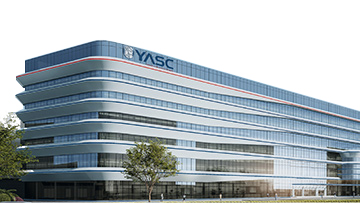
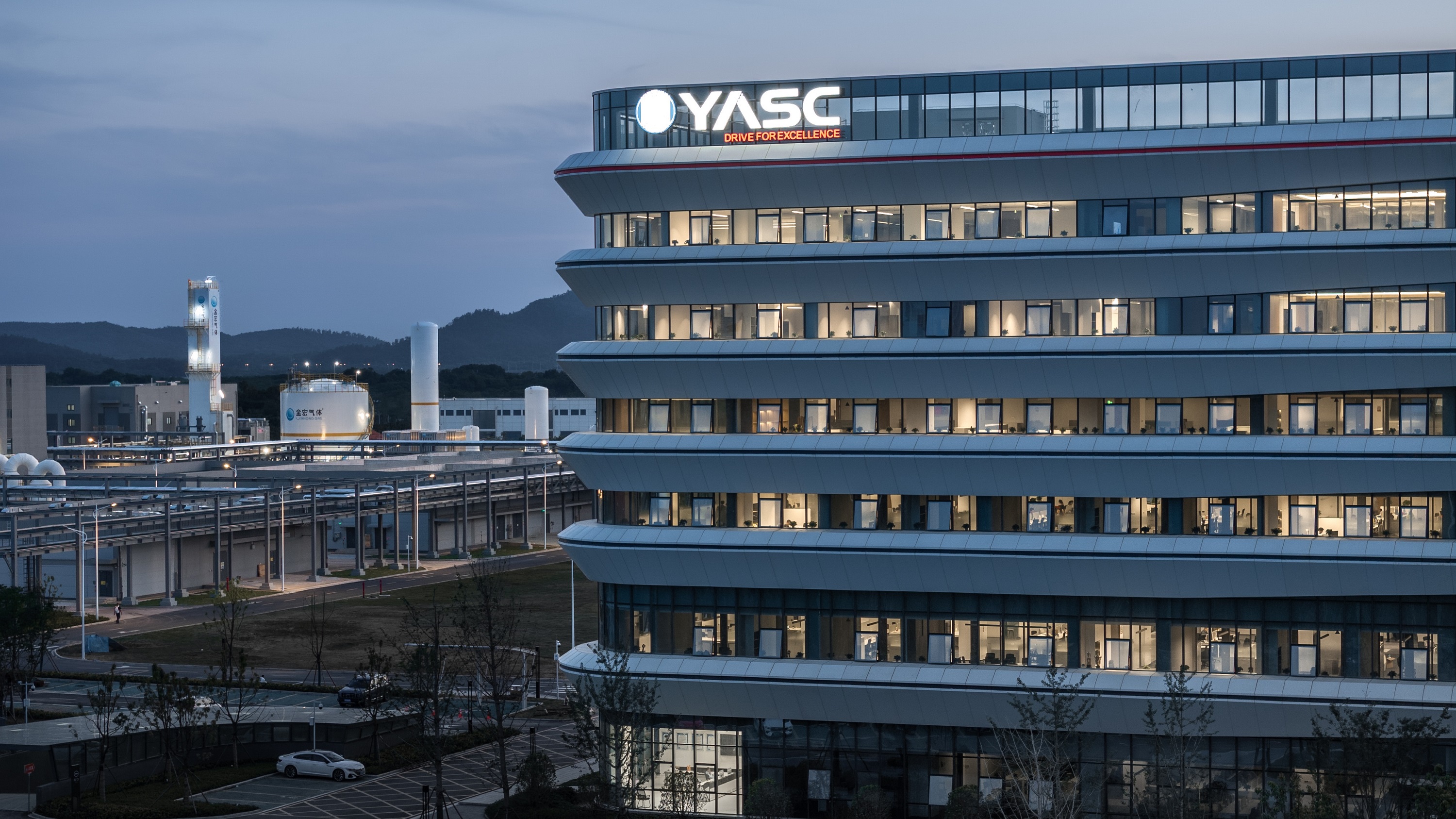
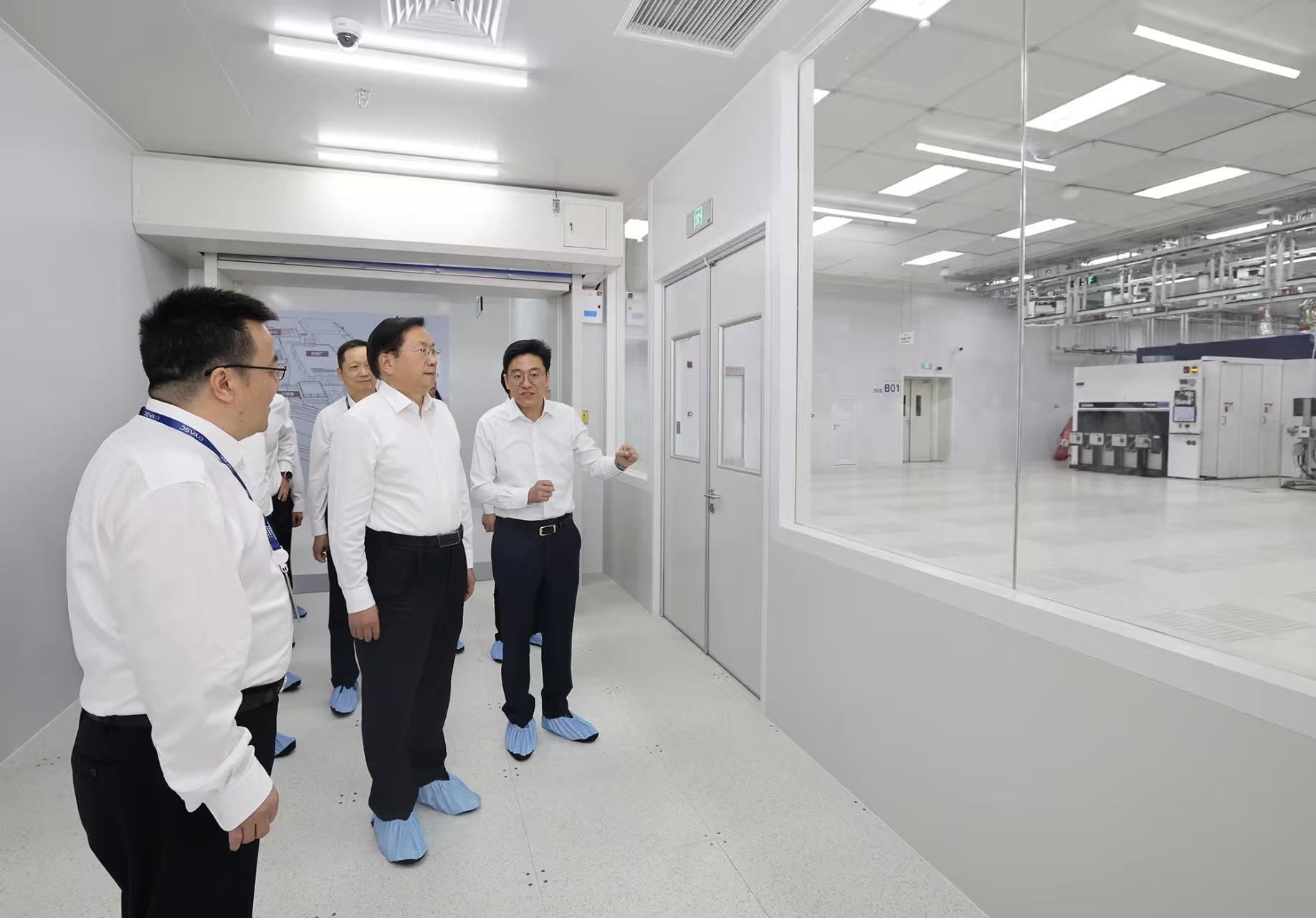
YASC, one of the earliest integrated device manufacturers (IDM) that have researched and developed SiC devices in China, has always attaches great importance to technology R&D and independent innovation, and also been active in providing the industry with public goods to drive the industry forward. Up to now, YASC has participated in a host of national and industry standards released, including five national standards (“Test method for resistivity of semi-insulating monocrystalline silicon carbide by contactless measurement”, “Polished monocrystalline silicon carbide wafers”, “Test method for surface defects on silicon carbide epitaxial wafers — Laser scattering method”, “Test method for thickness of silicon carbide epitaxial layer — Infrared reflectance method”, “Silicon carbide epitaxial wafers”) and many industry and association standards (such as “Test method for the content of metal elements on the surface of silicon carbide wafer — Inductively coupled plasma mass spectrometry”, “Acceptance specification for silicon carbide epitaxial wafer of high voltage power devices in the grid system”).
Looking ahead, YASC will continuously focus on SiC power semiconductor product research, development and manufacturing, constantly improve the enterprise standards system, actively participate in the development of relevant standards for the silicon carbide industry and application promotion at home and abroad, with the basic support of its high-level technology and talent advantages, and contribute to the high-quality industry development.