Three SiC MOSFET test and reliability standards including T/CASAS 042—2024 High-temperature gate bias test method for silicon carbide metal-oxide semiconductor field effect transistors (SiC MOSFETs), T/CASAS 043—2024 High-temperature reverse bias test method for silicon carbide metal-oxide semiconductor field effect transistors (SiC MOSFETs) and T/CASAS 044—2024 High-voltage high-temperature high-humidity reverse bias test method for silicon carbide metal-oxide semiconductor field effect transistors (SiC MOSFETs) were recently released at the opening ceremony of the 10th International Forum on Wide Bandgap Semiconductors (IFWS), and officially comes into force, with YASC participation in the development.
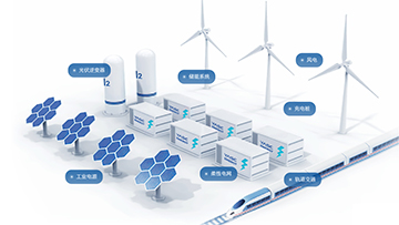
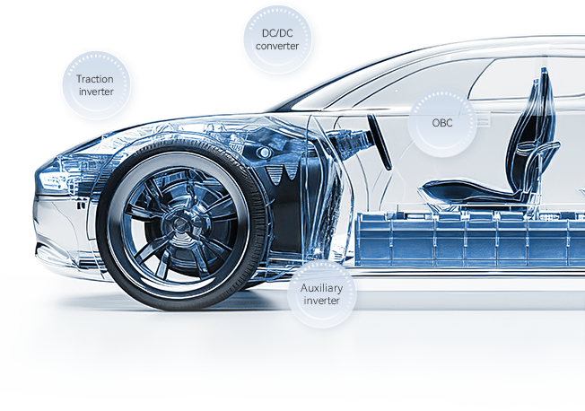
The silicon carbide metal-oxide semiconductor field effect transistors (SiC MOSFET) boast the characteristics such as high blocking voltage, high operating frequency, strong high-temperature tolerance, low on-resistance and low switching loss, and is widely used in high-frequency, high-voltage power systems. As power electronics technology continues to evolve, electronic devices that can operate under the requirements of high voltage, small heat dissipation volume and low loss are urgently needed in a growing number of fields like electric vehicle, photovoltaics, energy storage, charging station and aerospace. The series of SiC MOSFET test and reliability standards released by China Advanced Semiconductor Industry Innovation Alliance (CASA), with YASC participation in the development, aims to provide a set of scientific and reasonable test and evaluation methods for SiC MOSFET power devices, support product performance improvement, and promote high-quality development of the industry.

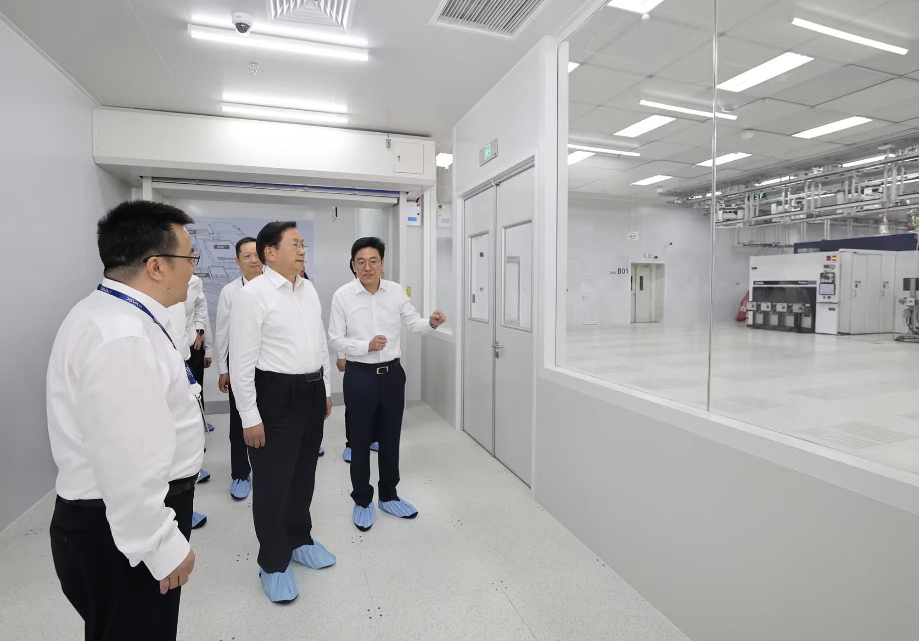
YASC, one of the earliest integrated device manufacturers (IDMs) that have researched and developed SiC devices in China, has attached great importance to technology R&D and independent innovation, and also actively undertaken the heavy lifting in industry development. Up to now, YASC has participated in a host of national and industry standards released, including five national standards (“Test method for resistivity of semi-insulating monocrystalline silicon carbide by contactless measurement”, “Polished monocrystalline silicon carbide wafers”, “Test method for surface defects on silicon carbide epitaxial wafers — Laser scattering method”, “Test method for thickness of silicon carbide epitaxial layer — Infrared reflectance method”, “Silicon carbide epitaxial wafers”) and many industry and association standards (such as “Test method for minority carrier lifetime in silicon carbide — Microwave photoconductive decay”, “Test method for the content of metal elements on the surface of silicon carbide wafer — Inductively coupled plasma mass spectrometry”, “Acceptance specification for silicon carbide epitaxial wafer of high voltage power devices in the grid system”).
Looking ahead, YASC will continuously focus on SiC power semiconductor product research, development and manufacturing, take an active part in developing relevant standards for the silicon carbide industry and application promotion at home and abroad, with the basic support of its high-level technology and talent advantages, and contribute to the high-quality industry development.